Smart Packaging, Smarter Chips
SK하이닉스 링크드인
SK hynix
May. 2025 -
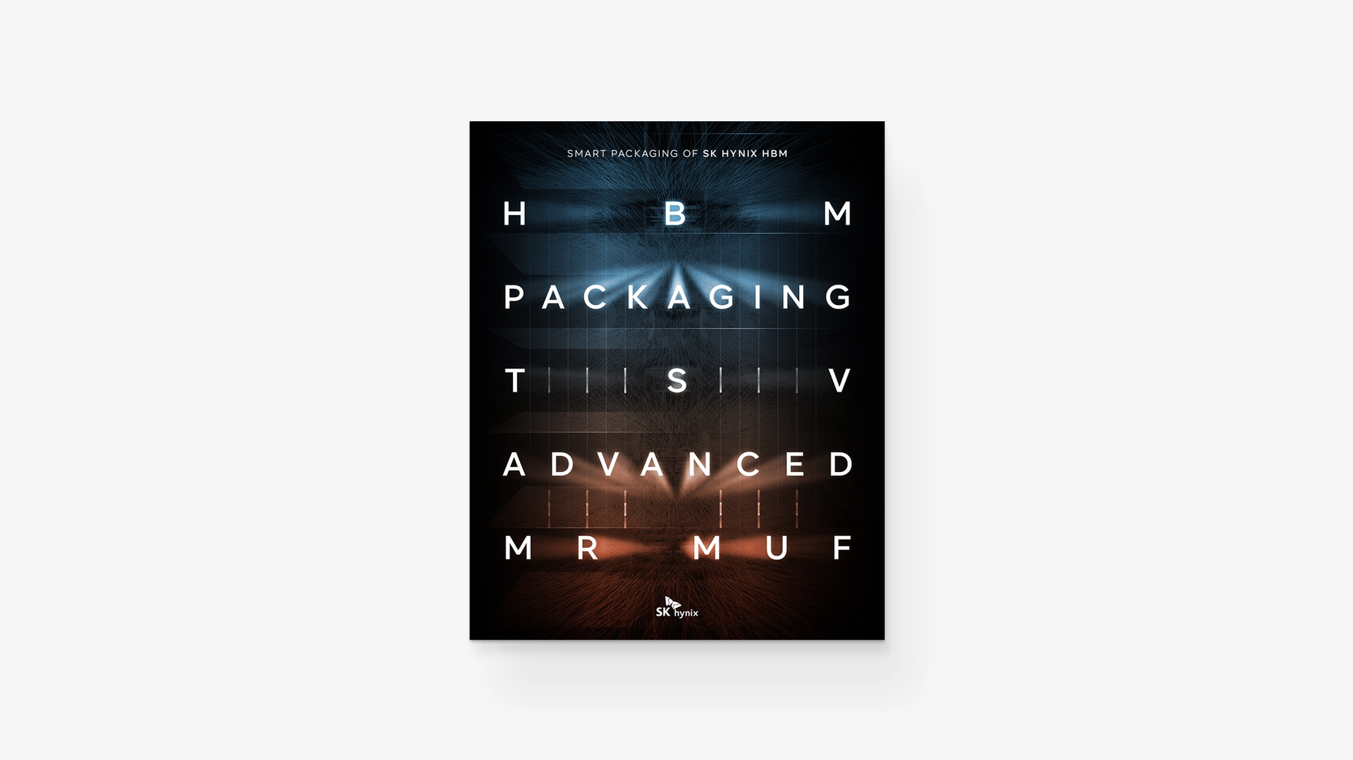
SK하이닉스의 HBM 패키징 기술을 위한 이번 프로젝트는 복잡한 반도체 기술을 시각적으로 해석하는 것을 목표로 했습니다. 정교한 타이포그래피와 첨단기술을 표현하는 디자인 요소들을 활용하여, 반도체 아키텍처의 조직적 복잡성을 반영하는 그리드 기반 레이아웃을 개발했습니다. 최종 결과물은 중앙의 구조화된 그리드와 분산·집중되는 입자 패턴을 통해 흐름과 정밀성을 동시에 표현하며, 기술적 정확성과 미적 매력 사이의 균형을 보여줍니다. 이러한 접근을 통해 전문가들이 쉽게 이해할 수 있으면서도 SK하이닉스의 기술 리더십을 효과적으로 어필하는 콘텐츠를 완성했습니다.
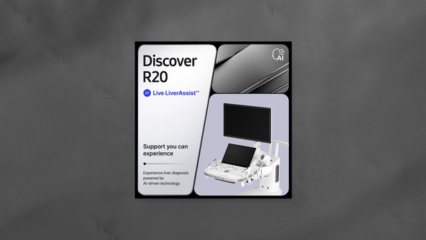
This project for SK Hynix aimed to visually interpret the sophisticated HBM packaging technology for LinkedIn content, translating complex semiconductor engineering into compelling professional narratives. Through refined typography and cutting-edge design elements, we developed a grid-based layout that mirrored the organized complexity of semiconductor architecture while maintaining aesthetic appeal. The final solution featured a central structural grid complemented by dispersed and concentrated particle patterns, effectively conveying both the technical flow and precision inherent in advanced memory packaging. This visual approach successfully balanced technical accuracy with professional engagement, creating content that reinforced SK Hynix's position as an industry leader while remaining accessible to LinkedIn's professional audience.
SK hynix - Smart Packaging, Smarter Chips
2025
Client SK hynix
-
Prain Global
Designer : Jiwon Kang